Voltage Notching
A notch is a condition when the magnitude of voltage decreases towards zero for a short period of time (usually in microseconds). Note that a voltage notch is different from a transient voltage event. Some type of transients also can cause the voltage to decrease sharply towards the zero-crossing axis. The key difference here is that voltage notching is a steady state condition whereas transients occur for only for brief instance when there is any momentary disturbance to the system. Examples of transients are lightning strike, capacitor switching etc.
Voltage notch is steady state condition meaning that it occurs always when the process that creates the notch (usually some type of SCR controlled device) is in operation. Voltage notch is created due to process known as commutation in Silicon Controlled Rectifiers (SCR). During the brief time when the current is transferred from one conducting SCR to another, a short circuit is created. The incoming SCR would have started conduction whereas the outgoing SCR will not have stopped conduction completely. This causes a phase-phase short circuit (for a very minute duration usually in micro seconds) enough to depress the voltage. This is the fundamental mechanism of voltage notch creation. Notch may occur at any point during the AC half cycle as the angle of commutation is not a constant value and keeps changing to meet the requirements of the load.
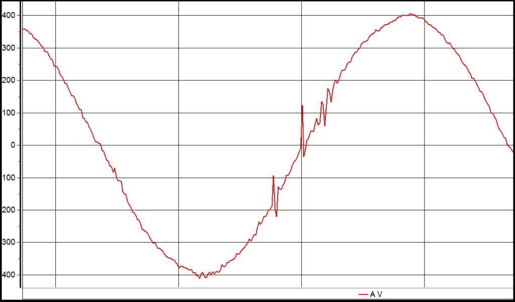
voltage notch
Which devices create notching?
Basically, any device that uses a phase controlled rectification in the front end circuit will cause some magnitude of voltage notch. Examples of devices that would cause notching are DC Drives, Controlled Rectifiers, SCR controlled AC heating circuits, Light dimmers etc.
Does VFD create notching?
The answer depends on what type of VFD is being used. Read below for the answer.
-
Modern low voltage VFD using pulse width modulated technology typically has diode front end circuit. Diode front end is an uncontrolled rectifier in the sense that the diode has no voltage control means. It just rectifies the AC input voltage. The simple answer is that if the VFD has a diode front end, then no voltage notching can occur.
-
Some manufactures larger VFD (>100 HP) sometimes uses a SCR soft charging circuit. This is to prevent large spikes of current to charge the DC bus on turn ON. These VFD will have SCR controlled front end which will charge the DC capacitors in a controlled manner (soft charge). Once the DC bus is charged, the SCR is gated ON all the time and the device now functions as a diode rectifier. During the brief time when the SCR is soft charging, we can expect to see some voltage notching. Note that this does not cause steady state voltage notching.
-
VFD that uses fully controlled front-end rectifier circuit using SCR will create steady state notching on the power supply voltage.
Problems caused by voltage notching
The interesting point to note here is that the device that creates the notch is usually not affected by the notching it creates. It is other devices that are connected to the same voltage source that are affected or disrupted due to notching. Some of the problems that could be created by voltage notching are:
-
Equipment that rely on zero crossing on the AC waveform may malfunction if the voltage notching is deep enough to create additional zero crossings on the voltage wave. A common example is when certain types of digital clocks run faster due to additional zero crossings.
-
The abrupt change in voltage due to notch excites natural frequencies of the electrical system. This creates additional non-characteristics harmonics to appear in the system voltage.
-
Possible radio interference due to presence of higher order frequencies radiating in the power network.
-
Voltage notching is very rich in high frequency harmonics and could damage sensitive logic and communication electronics in the facility.
-
Since notching creates high frequency harmonics (much higher than typical nonlinear device operation), filters connected in the same power system could experience additional current flow and could overload the filter circuits. These filters are usually EMI (Electromagnetic Interference) filters, Line filters etc.
-
Voltage notching can create additional losses in power factor capacitors and lead to elevated operating temperatures.
Standards for voltage notching.
Voltage notching standards are provided in the IEEE-519 standard. Notch depth and notch area limits are provided for:
-
Special Applications: Hospitals, Airports
-
General System
-
Dedicated System
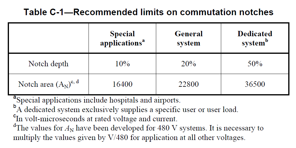
IEEE voltage notch limits
How to characterize Voltage Notch?
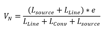
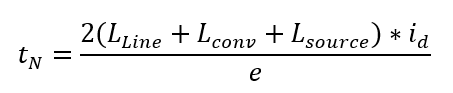
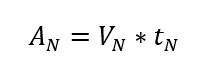
The key indices by which a voltage notch can be characterized are the notch depth (VN) and the notch area (AN). The figure below highlights the two parameters.
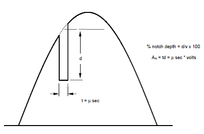
Voltage Notch Definition
Notch Depth: The depth of voltage notch or the magnitude of the voltage drop is strongly dependent on the ratio of the impedance between the converter (Lconv) and the source impedance (Lsource). Notch depth is also dependent on the firing angle of the converter which is usually not a parameter that the end user can control directly. The two parameters that the end user can adjust are the Lconv and Lsource, of which Lconv is the easiest to control.
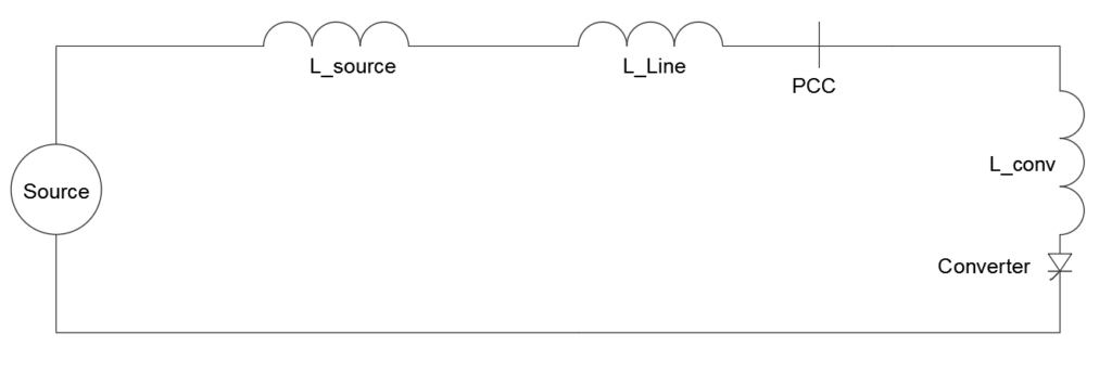
Lconv is the impedance between the converter and the point of common coupling (PCC). This could include any cables, isolation transformers, line reactors etc. installed on the supply side (line side) of the converter. Other way to look at Lconv is that this is the impedance of everything connected from the feeder breaker (or the point of common coupling-PCC) up to the converter terminals.
Line is the impedance of the system upstream of the PCC till the source. Usually this will be the impedance of connecting cables, transformers etc. Lsource is the impedance of the power grid.
For the system shown in the figure above, the notch depth can be calculated using:
The notch width can be calculated using:
From the equation for VN it can be noticed that for a given fixed value of Lsource and LLine, voltage notch depth can be reduced by increasing Lconv the converter inductance.
Notch Area: The area of the notch is a representation of the volt-seconds absorbed by the converter during the commutation process from the power source. Notch area is defined as the product of notch depth in volts and the notch width in microseconds. The unit of notch area is volt-micro seconds.
Notice from the equations above that adding too much impedance in front of converter will increase the notch width (tN) and hence notch area (AN). Usually a 3% reactance will be sufficient to reduce the notch depth to acceptable levels. Increasing the notch width too much also may create additional problems with the controller.
Lsource= Inductance of the source
LLine= Inductance of the line from source to the PCC
Lconv= Inductance between the converter and the PCC
e= Instantaneous voltage (Line-Line) just prior to the notch on the lines to be commutated
VN= Notch depth
tN= width of notch in microseconds
AN= Notch area in volt-micro-seconds
Id= converter DC current in amperes
Inspecting the equations for notch depth (VN) and notch width (tN), we can draw following conclusions:
-
Notch depth is reduced when the converter is connected to stiff source (LLine is small) and increases when connected to a weak source (LLine is large)
-
Notch depth is reduced when there is additional impedance between the converter and the source (Lconv).
-
The width of the notch increases with increasing any of the impedance (source, line of converter). Usually wider notch is a compromise that we will have to live with for obtaining smaller notch depth they are in inverse relationship. If too much impedance is added then the wide notch may create additional controller issues.
Preferred methods for reducing voltage notching
-
Apply the converter at a location with higher short circuit level (stiff source) as this will result in no to minimal notch depth depending on the converter size. A weak utility supply could result in relatively deeper voltage notch.
-
Add additional inductive impedance on the supply side of the converter. This could be an isolation transformer, line reactor. A 3% reactor is usually sufficient to reduce the voltage notch depth. Adding too much impedance (5% or more) will result in increase of notch area which may create additional controller issues. It is best to install this impedance immediately before the converter and not a location further away from the converter where it could feed other loads.